Materials and Processing

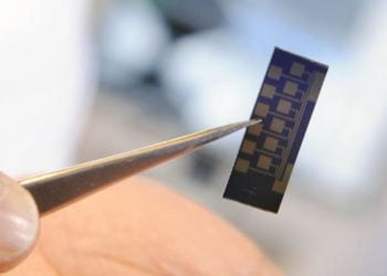
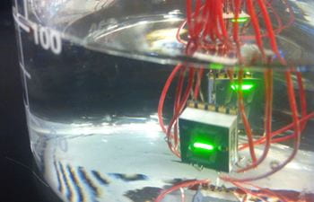
Fully integrated electronic systems on flexible substrates would have a wide variety of potential applications leading to a transformative and pervasive technology; from disposable computing devices and sensor systems to paper displays to clandestine listening and communication devices. While thin-film transistor technologies such as printed organic electronics provide the necessary flexibility and high-throughput manufacturing schemes, they are not typically energy-efficient nor offer the device performance necessary for many applications. Conventional silicon technology offers significant computational performance at relatively low power but does not have the necessary high-throughput manufacturing schemes. On the other hand, devices based on 2D materials such as transition metal dichalcogenides (TMDs such as MoS2) have the potential for energy-efficient performance equivalent to conventional semiconductors and can produce unique heterostructures, but are also flexible, strong, and can be fabricated using roll-to-roll (R2R) processes. Recent advances in materials and processing have led to complete R2R processing, using methods such as screen and inkjet printing and spray and slot-die coating, for example.

2D Materials

The Vogel group is performing broad-based research related to the synthesis, properties, and applications of 2D materials for flexible electronics.
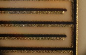
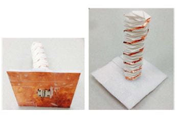
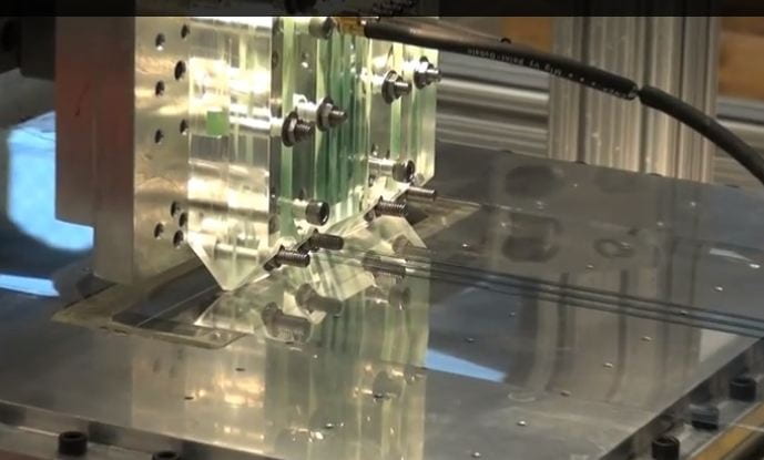
  • Large-area synthesis techniques have been developed for TMDs with properties equivalent to exfoliated materials.
  • Vertical tunneling heterostructures have been developed with unique electronic properties.
  • Piezoresistive strain sensors have been demonstrated using flexible MoS2 field-effect transistors made from a highly uniform large-area trilayer film.
  • Graphene biological and chemical sensors for flexible substrates have been demonstrated.
  • Aerosol Jet Printing

    With its state-of-the-art research facility for direct digital manufacturing, GA Tech currently focuses on aerosol jet printing (AJP) technology for printed electronics. The GTMI lab uses the latest model of the Optomec Aerosol Jet 300 System, a breakthrough additive technology that enables finer feature sizes than traditional inkjet and screen printing processes. AJP can be used to produce electronic devices from sensors and interconnects to 3D packaging and LEDs. The GTMI research team is utilizing AJP technology’s capabilities (print features of 10 microns width and sub-micron thickness) to fabricate miniature sensors for composite structural health monitoring and manufacturing processes monitoring that include temperature, pressure and gas sensors, organic transistors, RFID tags, high-frequency antenna, radar, and energy storage devices.

  • Batteries – Aerosol jet processes can create micro-meter size features on high roughness substrates for high-precision patterned printed electrodes for batteries and capacitors.
  • Sensors – The development of innovative printable, flexible, and embeddable sensors as well as ink material formulations for tailorable printed sensor performance.
  • Antenna – Achieving antenna reconfigurability by taking advantage of ‘‘origami-based’’ shape-changing enabled by a combination of inkjet printing and Additive Manufacturing Techniques (4D printing) on flexible materials.

4D Printing

A revolutionary way of depositing flexible smart materials through additive manufacturing is a process termed “4-D Printing” that uses a multi-material polymer printer to create printed active composites (PACs), which are 3-D printed, with an added fourth dimension being a shape change effect.

Current research by the Tentzeris group is devoted to utilizing 4-D printing to achieve partially self-actuated origami/kirigami inspired flexible reconfigurable antennas, resonators, and other RF structures. An Objet Connex 260 (Statasys, Edina, MN, USA) 3-D multi-material polymer printer has been used for the fabrication of a proof-of-concept preliminary flexible prototype. Droplets of a polymer ink are initially deposited at a temperature of around 70ºC and then UV photo-polymerized. Commercial inks TangoBlackPlus and VeroWhite are, currently, the most utilized materials for that purpose. The thermo-mechanical properties of the printed material’s matrix can locally be selected by adjusting the ratio of the two materials. Hinges for origami-type flexible folds are created using a matrix with a higher content of TangoBlackPlus, which employs a lower glass transition temperature than VeroWhite. The printed configuration of the structure, also called the ‘‘permanent’’ state, can be changed to a ‘‘temporary shape’’ by heating the hinges past the associated glass transition temperature and applying a small mechanical force. Once the object is cooled to room temperature, it maintains its ‘‘temporary shape.’’ Reheating the body past the glass transition temperature of the hinges triggers a return to the permanent state. Currently, our team is focusing on coupling this polymer depositing AMT with conductor-depositing AMTs, such as inkjet printing, in order to create fully additively manufactured flexible reconfigurable antennas.

Wearable and implantable electronics and sensors can benefit from these ‘‘4-D’’ structures, as they cause only minimal—if any—interference with motion. Other potential applications could also include, among others, health and contamination monitoring, artificial limb control, and exoskeletons. Wireless systems with requirements for arbitrary orientation cognitive radio systems, and real-time reconfigurable wireless systems (e.g., structural health monitoring ‘‘smart skins’’) could also benefit from this technology.

Extrusion Coating and Atomic Layer Deposition (ALD)

In the electronics field, printing a high-quality target pattern is of high importance. Since inkjet printing is a drop-on-demand approach, a coalescence of the drops can leave defects in the film, such as gaps and non-uniform thickness. The Harris Group has developed an Extrusion On-Demand approach that allows for changing the target pattern to be coated on a surface digitally. Additionally, Georgia Tech faculty are working to develop and implement customized slot-die coating as well as ALD and PECVD barrier films for the encapsulation and hermetic sealing of printed and assembled components.

  • Developing ALD ultra barrier layers to protect electronic devices from degradation due to normal environmental exposure.
  • Researching the coating of capacitive sensors for harsh environment electronics.
  • Testing both the fracture properties of coatings and adhesion with in-situ visualization to better understand their reliability for flexible electronics.

    Roll-To-Roll High-Speed Processing

  • The Harris Lab at Georgia Tech is investigating the use of advanced roll-to-roll(R2R) processing of flexible thin -films and substrates for use in the production of organic(O) and polymeric(P) photovoltaics.
  • Developing an advanced R2R processing method that allows for continuous in-line processing of tailored multi-layer OPVs or PPVs.
  • Implementing a hybrid processing tool that couples printing and coating technologies to enable continuous printing of discrete and/or non-discrete films in multiple layers.
  • Exploring the feasibility of using the proposed tool to continuously fabricate multi-layers of conductive polymers, with varying light-harvesting capability.

    Organic Photonics and Electronics

Center for Organic Photonics and Electronics (COPE) is a premier national research center that creates organic photonic and electronic materials and devices serving the information technology, energy, and defense sectors.

  • Combines a fundamental understanding of the essential chemical and physical phenomena in organic-based materials with advanced materials processing and device engineering.
  • Addresses underlying scientific problems relating to organic-based photonic and electronic materials and devices.
  • Employs faculty, research scientists, postdoctoral researchers, and students from groups with expertise in theory, synthesis, material science and characterization, device physics, and materials engineering.
  • Provides a multi-disciplinary research environment conducive to close collaboration with other Georgia Tech groups.
  • Encourages paradigm-shifting innovations by undertaking high-risk, high-payoff research.
  • Develops theory at multiple length scales that couples strongly to experimental studies.
  • Transfers technology to industry and government including commercializing technology by forming start-up companies.

Vogel Materials

Aerosol Jet Printing
Printed strain sensors array with interconnects
Printed strain sensor
Printed strain sensor on 3D printed flexible heart valve
Aerosol jet printed battery
Aerosol jet printed battery feature with line-widths less than 20 microns
Deployable origami antenna structure

Pasted Graphic

ALD Coated LEDs
ALD Coated LEDs that survive in phosphate-buffered saline solution for 6 months
Roll-to-Roll extrusion coding
Roll-to-Roll extrusion coding on flexible substrate


Center for Organic Photonics and Electronics
An introduction to the educational, research, and partnership activities of the Center for Organic Photonics and Electronics at the Georgia Institute of Technology — Link to video»

Center for Organic Photonics and Electronics
Professors Samuel Graham of Georgia Tech and Neal Armstrong of the University of Arizona comment on research at the Center for Organic Photonics and Electronics at the Georgia Institute of Technology — Link to video»

Faculty


  • Billyde Brown
  • Sam Graham
  • Tequila Harris
  • Bernard Kippelen
  • Dave McDowell
  • P. Markondeya Raj
  • Jud Ready
  • Manos Tentzeris
  • Eric Vogel
  • Ben Wang
  • ZL Wang
  • Gleb Yushin
  • Chuck Zhang