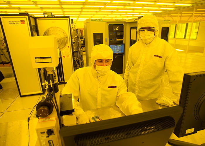
MICRO/NANO DEVICE FABRICATION LABShared User: Micro and Nano-Scale Device and Structure Fabrication18,500 square feet of semiconductor/MEMS cleanroom space and a fully equipped mask fabrication facility, as well as 5,000 square feet of biological cleanroom space rated up to Biosafety Level 2 in two buildings. |
ADVANCED ELECTRONIC PACKAGINGShared User: Advanced Electronic PackagingThese labs include Class 1000 to 100,000 cleanroom environments for the substrate fabrication, interconnect circuitry, and assembly processes needed for research integration and to provide functional sub-system test vehicles. |
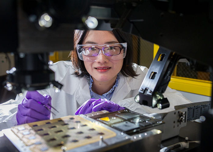
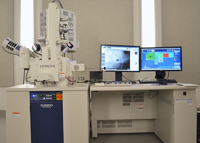
MATERIALS AND CHARACTERIZATIONShared User: Nanomaterials and Surface CharacterizationThese laboratories provide micro and nano-scale inspection, characterization, and measurement capabilities needed for organic and inorganic material, component, and device validation. |
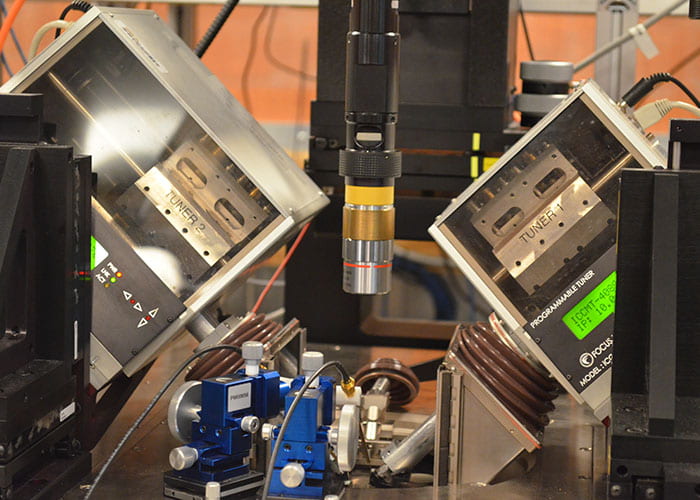
RF WAVE LABShared User: RF mm-wave and Photonic Testing & CharacterizationLocated in the Technology Square Research Building, this lab comprises a variety of RF, mm-wave, and photonics test beds and testing facilities.
|
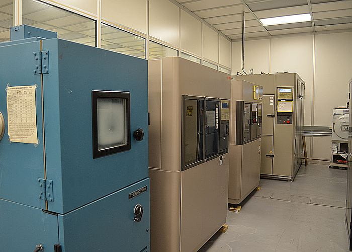
MECHANICAL RELIABILITY AND CHARACTERIZATIONShared User: Mechanical Reliability and CharacterizationThese laboratories offer a compendium of temperature, humidity, and mechanical stress systems used to reliability test packaging technologies. |
PI LABSParticipating Centers & Laboratory GroupsAs an umbrella program, Flex@Tech aims to be inclusive of all related Flexible Wearable Electronics programs at Georgia Tech. Associated Centers and Laboratory links are located here. |